Neon Ring Counters · Volume 9
High-Voltage Supplies — the Modern Way
Making a stiff 150–250 V ring rail from a 12 V brick with a boost converter — MC34063, a discrete MOSFET loop, a 555, a ready-made module, and a buildable current-limited bench supply
The traditional supply of Vol 8 makes its high voltage the way the tubes themselves were made — a mains transformer, a rectifier, a filter, and a cold-cathode VR tube shunting the rail to a regulated value — and there is a real satisfaction in feeding a neon ring counter from a supply that is itself a glowing gas-discharge device. But almost nobody building a ring counter today starts there. The modern answer to “where does the 150–250 V come from?” is a small switch-mode boost converter: a single inductor, a switching transistor, a fast diode, and a reservoir capacitor that take the 5–12 V you already have on the bench and pump it up to the rail the neons need, in a circuit the size of a postage stamp that runs cool and weighs nothing. It is cheaper, smaller, lighter, and — crucially — more stable than a transformer-and-VR-tube stack, and since Vol 7 identified supply stability as the single biggest lever on drift, “more stable” is not a nicety. This volume is the modern half of the supply story: why boost (and its cousin, flyback) is the right topology, a worked MC34063 design with every number shown, a discrete-MOSFET alternative for the builder who wants to see the whole loop, the minimalist 555 version, the buy-a-module shortcut, the handful of parts that keep the thing safe and steady, and finally a proper adjustable, current-limited, metered bench supply for characterising neon lamps. ⚠ Everything here still lives at 150–250 V behind a charged reservoir capacitor — lethal, and it does not announce itself; the full safety discipline is Vol 14, and you should have read it first.
9.1 Why a boost converter is the modern answer
A neon ring counter is an almost ideal load for a boost converter: it wants a high voltage but only a tiny current. A single lit lamp on Luc Small’s ring (Vol 4) draws about 800 µA; even a ten-stage ring with a buffer lamp or two, a feedback divider, and a bleeder rarely asks for more than a few milliamps total, because only one main lamp is ever lit at a time. So the supply’s job is to make 150–250 V at single-digit milliamps — an output power under two watts — from a low-voltage source. That is squarely in the comfort zone of the humblest boost converter, and it is why the whole heavy apparatus of Vol 8 (transformer, rectifier valve, choke, VR tube) is optional in the twenty-first century.
The boost converter earns its place for four concrete reasons. It is cheap — one
off-the-shelf inductor, one MOSFET, one diode, one controller chip, no custom-wound
transformer. It is small and light — no iron, no mains transformer, no glowing regulator
tube taking up a socket. It runs from whatever DC you already have — a 12 V wall-wart, a
9 V battery, a bench supply, a USB power bank through a small pre-boost — so the mains barrier
is handled by an approved external brick and your board never touches line voltage. And it is
electronically regulated: a feedback loop holds the rail flat against input droop and load
steps, which is exactly the stiffness Vol 7 ranked as the number-one drift mitigation. A ring
counter fed from a sagging supply drifts its Vs/Vm margins with every wobble of the rail;
a boost converter with a tight loop simply does not sag. The one thing a plain boost does
not give you is isolation — its input and output share a ground — but a ring counter has
no isolation requirement once a wall-wart provides the mains barrier, so that is a non-issue
here. Where you genuinely need isolation, or where the step-up ratio gets extreme (dekatrons
want +400–475 V, a 30:1 or 40:1 step from 12 V), the flyback converter — a boost whose
plain inductor is replaced by a coupled inductor with a turns ratio — is the tool, and it is
the same four functional parts with a transformer doing part of the voltage climb. For a
150–250 V ring rail, though, the plain boost is almost always the right and simplest answer,
and that is what the rest of this volume works through.
9.2 What the ring actually demands
Before designing a supply you must know its load, and a neon ring’s load is defined by two
numbers: the rail voltage it needs and the current it draws. The rail must clear the
worst-case striking voltage Vs of the lamps with margin, because the anode resistor
Ra drops tens of volts at operating current and because the striking event needs the full
rail momentarily across an un-conducting lamp (Vols 2, 4). The table collects the numbers
this dive has used, so the supply target is grounded in real builds rather than guessed.
Table 1 — 9.2 What the ring actually demands
| Build (from earlier volumes) | Tube | Rail | Lamp current | Note |
|---|---|---|---|---|
| Luc Small’s IN-3 ring (§2.4) | indicator neon, Vs ~75 V | 150 V | 800 µA/lamp | one lamp lit at a time |
| Dekker’s ZA1002 test ring (§2.2) | switching tube, Vs ~170 V | 185–250 V | ~1 mA | wide 60 V window |
| PA3FWM neon clock (§2.5) | indicator neon | +151/+157 V | ~1 mA/lamp | 8 counters, buffer lamps |
| Dekatron scaler (Vol 5) | glow-transfer counter | +400–475 V | a few hundred µA–mA | needs flyback / higher step |
For the worked example in this volume the target is a 180 V rail at ~10 mA — comfortably above the ~170 V striking voltage of a ZA1002-class switching tube, with generous headroom for the anode resistor and for a buffer lamp or two, and 10 mA gives ample overhead over the single-milliamp draw of the ring itself. That is an output power of 180 V × 10 mA = 1.8 W, which is a trivial ask for a boost converter and lets us size every part with a clear conscience. A ring built from cheap indicator neons on a 150 V rail (Luc’s numbers) simply sets the feedback divider lower; a dekatron rig needs the flyback of §9.1 to reach +400 V. The design method is identical — only the divider ratio and, for the dekatron, the topology change.
9.3 A worked MC34063 boost — 180 V from 12 V
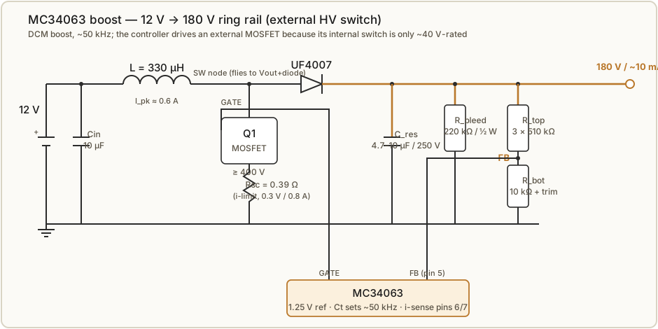
The MC34063 is the workhorse of hobby high-voltage supplies: a dollar chip with an on-chip 1.25 V reference, a comparator, an oscillator whose frequency is set by a single timing capacitor, a current-limit sense input, and a driver. It is slow (tens of kHz) and its internal switch transistor is only rated for about 40 V, so for a 180 V rail you do not use the internal switch to chop the inductor directly — you use the MC34063 as a controller and let it drive an external high-voltage MOSFET whose drain can safely fly up to the full output. That one substitution is the whole trick that turns a jelly-bean step-up chip into a nixie/neon HV supply, and it is how the boost stage in the owned ATMega nixie clock (from the sibling Clocks hub) is built.
Why the boost must run discontinuous. The textbook continuous-mode boost relates output
to input by duty cycle alone, Vout/Vin = 1/(1 − d), which for our step demands
d = 1 − 12 V/180 V = 0.93. A 93 % duty cycle crams all the output charge into the 7 % of
each cycle when the diode conducts; peak currents balloon and efficiency collapses. The clean
way out for a 15:1 step is discontinuous conduction mode (DCM): the inductor current
starts each cycle at zero, ramps to a peak, and is fully released into the output before the
next cycle begins. In DCM the controller sets the peak current and the frequency, not a
voltage-ratio duty cycle, and a 15:1 step is perfectly ordinary. An MC34063 boost naturally
behaves this way at light load.
Sizing it. Work the energy balance at a chosen switching frequency:
  Choose  f_sw = 50 kHz,  η ≈ 0.70 (a modest HV boost)
  P_out = 180 V × 10 mA = 1.8 W   →   P_in = P_out / η = 1.8 / 0.70 = 2.57 W
  Average input current  I_in = P_in / Vin = 2.57 W / 12 V = 0.21 A

  Energy stored/released per cycle  E = P_in / f_sw = 2.57 W / 50 000 Hz = 51 µJ

  With  E = ½·L·I_pk²  and a chosen  L = 330 µH:
        I_pk = √(2E / L) = √(2 × 51 µJ / 330 µH) = √(0.311) = 0.56 A  ≈ 0.6 A
So a 330 µH inductor at 50 kHz with a ~0.6 A peak switch current delivers the
rail. The timing capacitor sets the frequency through the MC34063’s on-time relation
Ct ≈ 4.0 × 10⁻⁵ × t_on (with Ct in farads and t_on in seconds); an on-time near 15 µs
gives Ct ≈ 600 pF, so a 470–680 pF timing cap lands in the right frequency band.
Three ratings fall straight out of the numbers:
- The inductor must not saturate at the ~0.6 A peak — pick a 330 µH part rated for ≥1 A saturation current (a small drum or toroid), and keep its DCR low enough that the I²R loss is negligible (0.6 A through 0.5 Ω is only 0.18 W).
- The switch MOSFET sees the full rail plus ringing on its drain when it opens — the node
flies to
Vout(180 V) plus the diode drop plus overshoot — so use a MOSFET rated ≥400 V (an honest 2× margin) that carries the ~0.6 A peak comfortably. An IRF840 (500 V) or similar is a cheap, robust choice. - The current-sense resistor
Rscsets the peak-current limit through the MC34063’s ~0.3 V (300 mV) sense threshold:Rsc = 0.3 V / I_pk,limit. To limit at 0.8 A (a bit above the 0.6 A working peak, so normal operation is never in limit),Rsc = 0.3 V / 0.8 A = 0.375 Ω → use 0.39 Ω. This resistor is the supply’s built-in overcurrent protection: a shorted output or a saturating inductor cannot pull more than the limit.
The fast HV rectifier. At 50 kHz an ordinary 1N4007 is useless — it is a 50/60 Hz rectifier whose slow reverse recovery dumps output charge backward as heat every cycle. Use a fast/ultrafast recovery diode rated well above the rail: the canonical choice is the UF4007 (1000 V, ultrafast), pin-compatible with the 1N4007 you must not use, and its 1000 V rating is luxurious insurance on a 180 V rail.
The reservoir capacitor holds the rail up between diode pulses and sets the ripple.
Rate it ≥250 V for a 180 V rail (never rate a cap at its working voltage), and size the
capacitance by the ripple you will tolerate: V_ripple ≈ I_load/(f_sw·C_res). With
C_res = 4.7 µF, V_ripple = 10 mA/(50 kHz × 4.7 µF) = 43 mV — about 0.02 % of 180 V,
invisible on the lamps. A 4.7–10 µF / 250 V film or high-voltage electrolytic is the
typical value; the upper end stiffens the rail against the load step a ring makes as its
buffer lamps and lit stage change.
9.4 Setting the output — the feedback divider
An unregulated boost lets the rail wander with input voltage and load, which for a ring
counter means its Vs/Vm margins wander with it — visible as erratic transfers or drift.
Every good supply therefore closes a feedback loop, and the mechanism is universal: a
resistor divider scales the high-voltage output down to the reference the controller can
compare against, and the loop modulates the switch to hold that divided sample equal to the
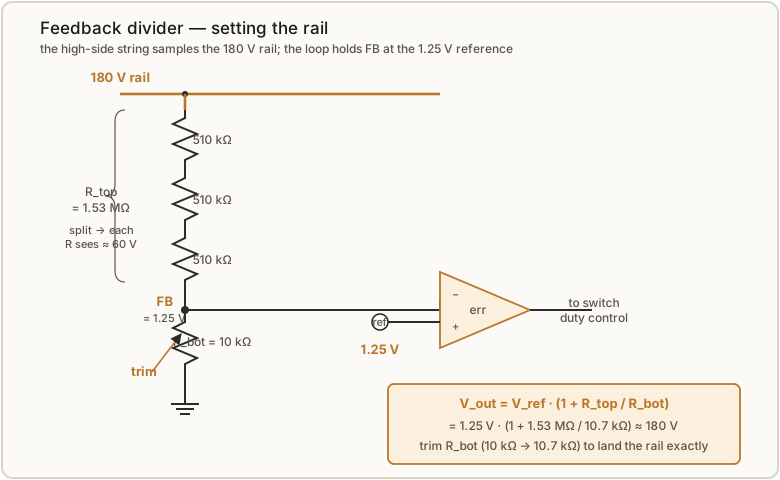
reference. For the MC34063 the reference is 1.25 V, and the output is
  V_out = V_ref × (1 + R_top / R_bot)

  Target 180 V with V_ref = 1.25 V:
        1 + R_top/R_bot = 180 / 1.25 = 144   →   R_top/R_bot = 143
  Choose R_top = 1.53 MΩ (as 3 × 510 kΩ in series):
        R_bot = R_top / 143 = 1.53 MΩ / 143 = 10.7 kΩ
  So R_bot = 10 kΩ fixed + a series trimmer to reach 10.7 kΩ:
        V_out = 1.25 V × (1 + 1.53 MΩ / 10.7 kΩ) = 1.25 × 144 ≈ 180 V
Two practical notes the bare formula hides, both of which matter more at 180 V than they would at 5 V:
- Divider current and dissipation are tiny. The string draws 180 V / 1.54 MΩ ≈ 117 µA, and the top resistor dissipates ≈ (180 V)²/1.53 MΩ ≈ 21 mW — negligible power, and a useful side-benefit is that this trickle helps bleed the reservoir (§9.8).
- ⚠ Voltage-rate the top resistor. A standard ¼ W axial resistor is rated for only
~200–250 V working voltage end-to-end, and a single 1.5 MΩ part across the full 180 V rail
is right at that limit with no creepage margin. Split
R_topinto three series resistors (3 × 510 kΩ) so each sees only ~60 V; this is standard high-voltage-divider practice and costs nothing.
Make part of R_bot a trimmer so the rail can be set precisely, and set it with the
ring’s actual load connected — the rail sags slightly under load, and a divider trimmed
open-circuit lands a few volts high. For a 150 V rail (Luc’s indicator-neon ring) the same
divider with R_bot re-trimmed to R_top/(150/1.25 − 1) = 1.53 MΩ/119 = 12.9 kΩ lands
150 V — one resistor changes, nothing else.
9.5 A discrete MOSFET boost with an op-amp feedback loop
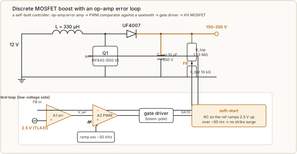
The MC34063 hides the control loop inside a chip. If you would rather see the whole loop — or want tighter, quieter regulation than the slow MC34063 gives — you can build the boost from a discrete HV MOSFET switch driven by a control loop you assemble yourself from an op-amp error amplifier and a PWM comparator. The power path is identical to §9.3: inductor, MOSFET, UF4007, reservoir, divider. What changes is the controller.
The loop works like this. The feedback divider samples the rail and presents a scaled copy
(say, ×1/72, so 180 V → 2.5 V) to the inverting input of an op-amp error amplifier
(A1); the non-inverting input holds a fixed reference — a 2.5 V TL431 shunt reference
is the clean choice. A1’s output, V_err, is the loop’s “how hard to push” command. That
command feeds a PWM comparator (A2) that compares V_err against a sawtooth ramp
from a ~50 kHz oscillator: the comparator’s output is high for the fraction of each cycle
that the ramp sits below V_err, so V_err sets the duty cycle. A small gate driver
(a totem-pole pair, or a dedicated driver chip) then swings the HV MOSFET’s gate hard between
0 V and ~12 V, because a 500 V MOSFET has appreciable gate charge and a lazy gate drive lets
it linger in its linear region and cook. Close the loop and the rail settles wherever the
divided sample equals the 2.5 V reference — V_out = 2.5 V × (1 + R_top/R_bot), the same
form as §9.4 with a 2.5 V reference instead of 1.25 V.
Why bother, when the MC34063 does all this in one package? Three reasons. A discrete loop can switch faster and with a tighter, better-compensated error amplifier, giving lower ripple and better load regulation — the stiffness Vol 7 wants. It is transparent: every node is a test point, which makes it the better teacher and the easier thing to debug. And it lets you add a proper soft-start trivially (§9.8) by putting an RC on the reference so the 2.5 V ramps up over ~50 ms at power-on, bringing the rail up gently instead of slamming it to 180 V and hammering the reservoir and the freshly-struck lamps. The MAX1771 and similar purpose-built boost controllers (which drive an external MOSFET and regulate against a 1.5 V reference) are the productised middle ground — most of the discrete loop’s virtues in one chip — and are the quiet favourite for a stiff, low-ripple rail without a module.
9.6 The 555 boost — for the minimalist
If a chip and an inductor is one part too many, the classic hobbyist hack strips the loop out
altogether: a 555 timer free-running as an astable at tens of kHz drives a MOSFET’s gate
directly, chopping current into a boost inductor, with a UF4007 and a reservoir cap on the
output exactly as before. A 555 astable at ~50 kHz uses the familiar f ≈ 1.44/((R_A + 2R_B)·C)
with, say, R_A = 1 kΩ, R_B = 12 kΩ, C = 1 nF, giving f ≈ 1.44/(25 kΩ × 1 nF) ≈ 58 kHz;
tune R_B for the frequency and duty that make your rail.
The catch is regulation — or the lack of it. A bare 555 boost is open-loop: the output climbs until the inductor’s energy per cycle balances the load, and it moves with input voltage, load current, and temperature. The usual fixes are crude but effective. The simplest is a zener (or a series string of zeners) clamping the output at, say, 180 V — the boost runs slightly hot and the zeners bleed the excess, wasteful but dead simple. A cleaner fix adds a transistor sketch of feedback: sample the rail with a divider, and when it exceeds the set point, pull the 555’s reset or control-voltage pin to throttle the drive — a one-transistor loop that turns the open-loop boost into a roughly-regulated one. Either way the 555 boost is the least-regulated of the family: it is a fine way to get a ring lit on the bench for the first time and to learn the topology hands-on, but for a ring that must run flicker-free for a year, close the loop properly with the MC34063 of §9.3 or the discrete loop of §9.5. Its virtue is that it is built entirely from the junk box, and there is genuine value in watching a 555 — the most abused chip in electronics — make 180 V out of nothing.
9.7 The lazy (and often smart) option — a ready-made nixie-PSU module
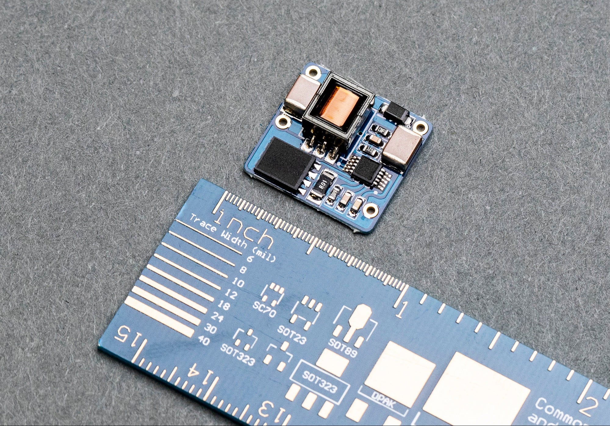
For a builder who wants a ring counter and not a power-supply project, the pragmatic answer is to buy a finished nixie HV module and treat it as a black box that eats 12 V and makes 180 V. These postage-stamp boards — the NCH8200HV class is the archetype — carry the inductor, the switching MOSFET, the fast rectifier, the reservoir cap, the feedback divider, and an output-set trimmer, all in a tested package the size of a large stamp, delivering ~170–200 V at ~20–25 mA from a 9–12 V input. They are exactly the boost of §9.3, done and trimmed for you, and they are what most commercial nixie kits ship. For a neon ring they are ideal: a ring’s few-milliamp draw is a fraction of a module’s rating, so it runs cool and lightly loaded, and you set the rail with the on-board trimmer (with the ring connected, per §9.4). The only real cost is that a module is a box you cannot tune beyond its trimmer and cannot easily probe — fine for a finished build, less good when you are learning or when you want an unusual rail voltage. ⚠ Note that a module’s output is just as lethal as a home-built one, and many ship without a bleeder across their reservoir — fit one yourself (§9.8).
9.8 The essentials that keep it safe and stable
A boost converter that merely reaches 180 V is not yet a good supply. Four details separate a rail you can trust a ring counter to for a year from one that flickers, drifts, or bites you.
Output current limiting. The current-sense resistor of §9.3 (Rsc = 0.3 V/I_pk,limit) is
not optional dressing — it is the supply’s protection against a shorted output, a saturating
inductor, or a lamp that arcs over. A boost with no current limit that sees a short drives its
switch to maximum forever and destroys the MOSFET or the diode; the sense resistor caps the
peak current cleanly. On the discrete loop of §9.5, add a second comparator watching the same
sense node and pulling down the gate drive when the limit is hit. Always bench a boost
supply with its current limit proven before you trust it to a load.
The mandatory bleeder resistor. ⚠ The single most important safety part in this volume
costs a few cents: a bleeder resistor permanently across the reservoir capacitor, so that
when you switch off, the stored charge drains to a touch-safe level on its own, in a known and
bounded time, instead of lying in wait. Without it the reservoir holds 180 V for minutes —
the feedback divider alone (1.54 MΩ) bleeds a 4.7 µF cap only slowly (τ = 1.54 MΩ × 4.7 µF = 7.2 s, so ~20 s to genuinely safe) — and a builder who switches off and reaches in ten
seconds later gets the full jolt. Size it as a trade between discharge speed and wasted power:
  Discharge is RC:  V(t) = V0 · e^(−t/RC),  τ = R·C
  Choose  R_bleed = 220 kΩ  across  C_res = 10 µF:
        τ = 220 kΩ × 10 µF = 2.2 s
  Time to fall from 180 V to a touch-safe < 50 V:
        t = τ · ln(180/50) = 2.2 s × ln(3.6) = 2.2 × 1.28 = 2.8 s
  Continuous power wasted while running:
        P = V²/R = (180 V)²/220 kΩ = 0.147 W  →  use a ½ W part
So 220 kΩ / ½ W bleeds the rail from 180 V to under 50 V in under 3 seconds and wastes only 0.15 W keeping the ring running — a good balance. Push it higher (470 kΩ) to waste less but bleed slower; lower (100 kΩ) to bleed in a second at 0.32 W. Size the wattage for the continuous V²/R dissipation, not a fraction of it — a ¼ W part at 0.15 W runs hot; ½ W is the honest choice — and ⚠ split it into series resistors if a single part’s voltage rating is marginal. The bleeder is not optional and it stays fitted in the finished build.
Soft-start. Slamming a cold reservoir cap from 0 V to 180 V at power-on draws a large inrush through the diode and switch, and it hits a ring’s lamps with the full rail before anything has settled. A soft-start ramps the rail up over tens of milliseconds. The clean way, on the discrete loop of §9.5, is an RC on the reference so the 2.5 V set-point rises over ~50 ms — the loop follows it up gently. On an MC34063 you can approximate soft-start with an RC that slowly raises the FB set-point, or accept the inrush and simply size the switch and diode for it. Either way, a gentle bring-up is kinder to the reservoir cap, the semiconductors, and freshly-struck lamps than a hard slam.
Ripple and regulation — the drift connection. Vol 7 ranked a stiff, regulated supply
as the number-one lever against drift, and this is where that lever lives. A neon lamp strikes
at Vs and the ring’s whole timing margin is Vs − Vm, only ~12–20 V for indicator neons; if
the rail ripples or sags by even a few volts, it walks the lamps around inside that narrow
window and shows up as jittery or unreliable transfers. Two things keep the rail stiff:
adequate reservoir capacitance (the §9.3 sizing keeps ripple to tens of millivolts) and a
tight feedback loop (a well-compensated discrete loop or a MAX1771 over a sloppy 555). If
a ring’s transfers get erratic as the display pattern changes — more lamps’ worth of current
drawn on some counts than others — suspect the rail breathing under the load step before you
suspect the tubes. A regulated boost with a stiff reservoir holds the rail flat through the
load change, and the ring’s margins hold with it. This is the concrete payoff of choosing the
modern supply: its electronic regulation is drift mitigation.
9.9 A buildable bench supply for neon experiments
Everything above makes a fixed rail for a finished ring. But the work that precedes any ring
— binning lamps by Vs/Vm (Vol 3), burning them in (Vol 11), probing the V–I curve
(Vol 2) — wants something different: an adjustable, current-limited, metered high-voltage
bench supply you can dial from below the lowest striking voltage to above the highest, with a
current limit low enough to keep a lamp on its normal-glow plateau instead of letting it run
away into an arc. This is the most useful single instrument for neon work, and it is a
weekend build. The design target: ~80–250 V adjustable, current-limited from ~0.1 mA to
~20 mA, with voltage and current both metered.
Architecture. The clean approach is two stages: a fixed boost pre-regulator that
makes a raw rail a little above the maximum output (≈ +280 V), followed by a series-pass
linear post-regulator — an HV MOSFET in series with the output, its conduction controlled by
an op-amp loop — that drops the raw rail down to the adjustable, clean, low-ripple output. The
boost does the voltage climb; the linear pass stage does the regulation and adjustment,
giving an output far quieter than a bare boost (no switching ripple on the output at all) and
trivially adjustable with a pot. It costs a little efficiency — the pass MOSFET dissipates
(V_raw − V_out) × I_out, at most (280 − 80 V) × 20 mA = 4 W — which is why the raw rail
sits only ~30 V above the maximum output rather than at some wasteful height, and why the pass
MOSFET wants a small heatsink.
The two control loops. Two op-amps share command of the pass MOSFET’s gate, and the lower-demanding one always wins — the standard constant-voltage / constant-current bench-supply trick:
- The voltage loop (
A_V) compares a ÷100 sample of the output (a 1 MΩ-over-10 kΩ divider, the 1 MΩ split into series parts for voltage rating) against an adjustable reference set by the front-panel VOLTAGE pot (a 10-turn pot across a 2.5 V TL431 gives a 0–2.5 V set → 0–250 V out). When the output is below the set point,A_Vturns the pass MOSFET on harder. - The current loop (
A_I) senses the drop across a low-side sense resistorR_sin the output return and compares it to the CURRENT pot set point. When the load current reaches the set limit,A_Isteals gate drive from the pass MOSFET, holding the current constant and letting the voltage fall — exactly what you want when a lamp strikes and you need to hold it at a defined current on its glow plateau.
Their outputs are wired-OR onto the gate node (each can only pull the gate down, toward less
conduction; a resistor from the raw rail pulls it up), so whichever loop demands the lower
output governs. Below the current limit the supply is a clean adjustable voltage source; at
the limit it folds into a constant-current source. For neon work R_s = 100 Ω gives 1 V at
10 mA — enough for the op-amp to act on — and a range switch selecting R_s = 100 Ω
(mA range) or 10 kΩ (µA range, for measuring striking currents) lets the same supply hold a
lamp at anything from a few microamps to tens of milliamps.
Metering. A small digital panel meter (0–300 V range, reading the output directly or
through a 1:1000 divider) shows the set and actual voltage; an analog µA/mA meter in the
return — or a second digital panel meter across R_s scaled to current — shows the draw. The
analog meter earns its keep here: watching the needle is the fastest way to see a lamp strike
(current jumps as it breaks down) and to find the maintaining current as you back the voltage
down. ⚠ Fit the bleeder across the output reservoir as always — a bench supply is switched
on and off constantly and is exactly where an un-bled reservoir catches you; a 100 kΩ/2 W part
across a 22 µF output cap gives τ = 2.2 s and dissipates (250 V)²/100 kΩ = 0.6 W at full
output, so a 2 W part runs cool.
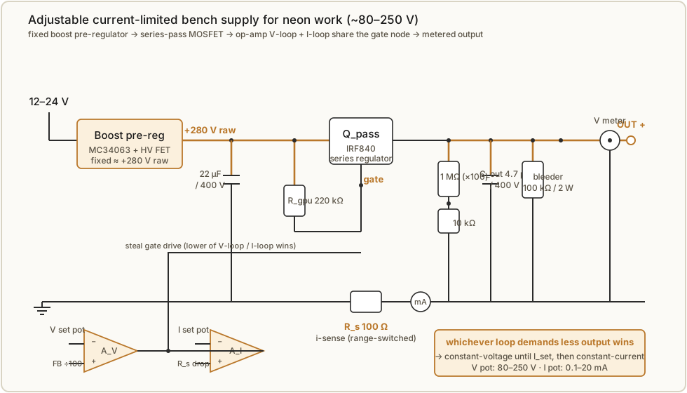
BOM notes. The parts are ordinary and cheap; the discipline is in the voltage ratings.
Table 2 — 9.9 A buildable bench supply for neon experiments
| Block | Part | Notes |
|---|---|---|
| Boost pre-reg | MC34063 + IRF840 + 330 µH + UF4007 | §9.3 design retargeted to ~+280 V (divider ratio only) |
| Raw reservoir | 22 µF / 400 V | rate well above the 280 V raw rail |
| Series pass | IRF840 (500 V) N-MOSFET | on a small heatsink; dissipates up to ~4 W |
| Gate pull-up | 220 kΩ from raw rail | lets the loops pull the gate down toward cut-off |
| Error amps | dual op-amp (e.g. TL072/LM358), 2.5 V TL431 ref | run from a low-voltage housekeeping rail |
| V sense divider | 1 MΩ (3 × 330 kΩ series) : 10 kΩ | ÷100; split the top for voltage rating |
| Set pots | 10-turn 10 kΩ ×2 (VOLTAGE, CURRENT) | front-panel; multi-turn for fine setting |
| Sense resistor | 100 Ω (mA) / 10 kΩ (µA), range-switched | 1 % metal-film, ≥¼ W |
| Output cap | 4.7–22 µF / 400 V | small = fast response; large = stiffer, slower bleed |
| Bleeder | 100 kΩ / 2 W | ⚠ mandatory; τ ≈ 2.2 s from 250 V |
| Meters | digital panel V-meter (0–300 V) + analog µA/mA meter | analog needle best for watching strikes |
| Input fuse | 1 A slow-blow on the 12–24 V input | a shorted switch is a near-dead-short across the brick |
A supply built to this pattern will bin a box of neons, ramp a lamp’s V–I curve, hold a tube at a chosen glow current for burn-in, and — dialled to a fixed 150–200 V — run a finished ring directly. It is the one piece of high-voltage test gear this whole dive most rewards building, and it folds the entire volume’s lessons (a boost front end, a regulated adjustable output, a current limit, a bleeder, and safe metering) into a single instrument. ⚠ It is also a live 150–250 V source with a charged reservoir the moment it is powered — treat every terminal as lethal, keep one hand behind your back when probing, and prove the rail discharged before you reach in. The full discipline is Vol 14.
9.10 9.x References
- R. Dekker (dos4ever), “A Neon Ring Counter” / Ring Counter Variations — https://www.dos4ever.com/ring/ring.html (the 185–250 V ZA1002 ring supply target).
- L. Small, “Neon Ring Counters” (2016) — https://lucsmall.com/2016/10/08/neon-ring-counters/ (the 150 V rail and 800 µA-per-lamp load numbers).
- P.-T. de Boer (PA3FWM), “A clock using neon lamps as logic elements” — https://www.pa3fwm.nl/projects/neonclock/ (+151/+157 V rails; the supply-stability lesson).
- ON Semiconductor, MC34063A DC-DC converter control-circuit datasheet — 1.25 V reference,
~0.3 V current-sense threshold (
Rsc = 0.3 V/I_pk), timing-capacitor relation, boost configuration. - Maxim Integrated, MAX1771 step-up controller datasheet — 1.5 V reference, external-MOSFET current-mode boost (the tighter-regulation alternative of §9.5).
- Vishay, UF4007 ultrafast 1000 V rectifier datasheet — the fast HV diode that replaces the too-slow 1N4007 in a switching supply.
- Omnixie / NCH8200HV-class nixie HV module documentation — 12 V → ~170–200 V trimmer-set boost module (the drop-in path of §9.7).
- J. B. Dance, Electronic Counting Circuits (1967) — in the site’s reference library (canonical text; supply/regulation practice cross-referenced from Vol 8).
- Cross-references within this dive: Vol 2 (
Vs/Vm, V–I curve), Vol 4 (ring load, anode resistor), Vol 5 (dekatron +400–475 V rails), Vol 7 (supply stability as the top drift lever), Vol 8 (the traditional VR-tube supply), Vol 11 (the burn-in jig this bench supply feeds), and Vol 14 (the ~100–450 V safety discipline).
Comments (0)