CubeSat Simulator · Volume 4
The Schematics — Vol 4
The Schematics — Vol 4
Introduction
This volume reads the v2.1 board schematics circuit by circuit. The three PDFs are reproduced here as figures and annotated; the goal is that you can follow every functional block — compute, RF, sensing, power — from net to net. The source files are the project’s own EAGLE/CAD exports in the GitHub hardware/v2.1 folder.1
License / attribution. Each board’s title block reads ”© CC-BY-NC-SA+ 2019–2024 AMSAT — KU2Y / KI6ZUM / WD6DRI — CubeSatSim.org.” These schematics are reproduced under CC-BY-NC-SA: attribution required, non-commercial, share-alike. Credit AMSAT in any reuse.
How to read these. The CubeSatSim schematics use named nets rather than drawing every wire — e.g. PI_RF, FM_RF, FILTER_OUT, PICO_SDA/SCL, BATT_SW, AUDIO_OUT, PTT, PD. A signal appears wherever its label appears. The walk below follows those names.
1. Main board (STEM Payload Board)
The full Main board schematic sheet (PDF) is in the Schematics ▾ launcher at the top of this reader. Schematic: AMSAT CubeSatSim v2.1 (CC-BY-NC-SA), alanbjohnston/CubeSatSim. The PCB top render below cross-references it.
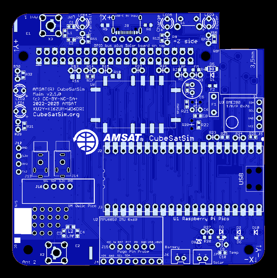
The Main board is the whole avionics suite on one PCB. Five functional blocks:
1a. Compute
- U1 — Raspberry Pi Pico (RP2040). The payload MCU. Its GPIO carries the I²C sensor bus (
PICO_SDA/PICO_SCL), a second I²C (PICO_SDA2/SCL2, via the optional U4 SparkFun Qwiic adapter), the FM-module serial (TX2/RX2),PTT,PD(power-down),AUDIO_OUT, the push-buttonPB, and the status-LED drives. - Raspberry Pi Zero (2) mounts on the 20×2 stacking header J1. Shared nets include
PI_RF,PI_TXD/PI_RXD,PI_LED1/2,PI_3V3. A nice detail: the Pico senses 3.3 V on a Pi pin to detect whether a Pi Zero is present — so the same board runs either as a Pi-hosted satellite or as a standalone Pico STEM payload.
1b. RF chain — the downlink
This is the heart of the board. Signal flow: audio in → FM module → attenuator → low-pass filter → SMA antenna.
- Transmitter module — U6 (SR105U), with U7 (DRA818/SA818) as a legacy alternative. The board has footprints for both, but the as-built radio is U6, an SR_FRS-family 0.5 W UHF FM module marked SR105U (“U” = UHF; the pin-compatible SR105V is the VHF sibling AMSAT uses for APRS balloon payloads). The current build instructions consistently mount “the SR_FRS board U6,” and the firmware self-identifies it (a 1 kΩ in R3/R4 ⇒ SR105U fitted). U7 is the older DRA818/SA818-class walkie-talkie module — in the v2.1 BOM it carries a “check availability” note (it became hard to source, which is why the SR_FRS is now default). Either module exposes the same control pins:
PTT,PD,MIC_IN(audio),H/L(high/low power select),VBAT,ANT, andRXD/TXDfor serial frequency/config. (One trap: the U7 schematic symbol is labeled “DRA818V”, but the board is a UHF design — “UHF low-pass filters”, “1k in R1/R2 ⇒ UHF LPF present.” If you ever populate U7 for the 434.9 MHz downlink you need the UHF variant, DRA818U/SA818U — the “V” is just the generic symbol/value, not an endorsement of the VHF part.) - Audio generation. Telemetry/SSTV audio is produced by PWM on the Pico/Pi, then smoothed by an RC low-pass filter (the design is credited in-schematic to a hackster.io “PWM audio on Pi Pico” technique). The filtered
AUDIO_OUT → FILTER_OUTfeeds the module’sMIC_IN. This is the bridge from digital bits to an FM-modulated tone stream (AFSK/FSK/SSTV). - Output attenuator. A 17 dB pi-attenuator drops the module’s ~500 mW to about 10 mW for safe, legal low-power demonstration (the schematic even cites a pi-attenuator calculator). Bridge JP2 to bypass it; for high power (~500 mW), cut JP11 and bridge JP2.
- Output filtering + antennas. Each of the two SMA female jacks (
X2= Antenna 1,X3= Antenna 2) sits behind a UHF low-pass filter built fromL1/L2 = 13 nHandC1=18 pF, C2=16 pF, C3=18 pF, C4=16 pF(LPF design credited to Randy Standke, KQ6RS). Solder-jumpers select one antenna or both. This LPF is the “integrated 433 MHz filter” the AMSAT papers refer to — it cleans up the FM module’s harmonics so the downlink is spectrally clean.
1c. Sensors (telemetry payload)
- U2 = MPU6050 — 9-DOF IMU (accelerometer + gyroscope) with on-chip temperature, on header J4, I²C.
- U3 = BME280 — temperature / barometric pressure / humidity, on header J5, I²C.
- D3 = 1N4148 — a diode used as a simple temperature sensor (net
TEMPERATURE); a forward-biased junction’s voltage is a clean temperature proxy.
1d. Power & charge
- Inputs: USB-C via
J8(SparkFun USB-C breakout) orJ9(direct USB-C); battery via theBATT/BATT_SWnets. - RBF (Remove-Before-Flight) switch gates the battery into the system — pulling it “launches” the sim. Bridge if not used.
- F1 = RHEF100-2 PTC resettable fuse protects the battery path (it “replaces D4 in earlier versions”; bridge JP10 if omitted).
- Charging is Pico-managed off the USB-C 5 V rail — bridge JP1 to enable the Pico to power and charge the battery. (There is no dedicated charger IC such as the CN3058 used in older revisions.)
- Steering/protection:
D1 = BYW27-400,D2/D10 = 1N5817Schottky, optional 5V1 1 W Zener (DNI).
1e. User I/O
- S1 = the mode push-button (
PBnet) — short presses cycle transmit modes. - Five status LEDs —
LED1White,LED2Yellow,LED3Green,LED4Blue,LED5Red — driven by Pi/Pico to show power/charge/transmit state and the selected mode. (The exact color/blink-to-mode mapping is operational detail covered in Vol 5.)
2. Battery board
The full Battery board schematic sheet (PDF) is in the Schematics ▾ launcher at the top of this reader. Schematic: AMSAT CubeSatSim v2.1 (CC-BY-NC-SA), alanbjohnston/CubeSatSim. The PCB top render below cross-references it.
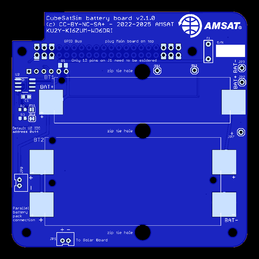
A deliberately simple board: hold the cells, measure them, protect them.
- Cells: 3× AA NiMH — two single-AA holders (
BT1) or one dual holder (BT2);JP13/JP14+ aBH3AAPCholder as a fallback. Three NiMH cells ≈ 3.6 V nominal, ~4.0–4.2 V freshly charged. NiMH (not lithium) keeps the kit classroom-safe. - Telemetry: U2 = INA219AIDR — a high-side voltage + current monitor (the circuit follows Adafruit’s INA219 reference design) reading battery voltage and current through a 0.1 Ω shunt (R1);
R2/R3 = 10 kΩare I²C pull-ups. NetsBATT_IN/BATT_OUT. - I²C addressing: the primary battery is at 0x44, a secondary at 0x45 (bridge JP11) — so multiple battery boards can be chained and individually monitored.
- Protection:
F1 = PTCfuse (cut JP5 if used);JP4bridges out the RBF if the switch lives only on the Main board.
3. Solar board
The full Solar board schematic sheet (PDF) is in the Schematics ▾ launcher at the top of this reader. Schematic: AMSAT CubeSatSim v2.1 (CC-BY-NC-SA), alanbjohnston/CubeSatSim. The PCB top render below cross-references it.
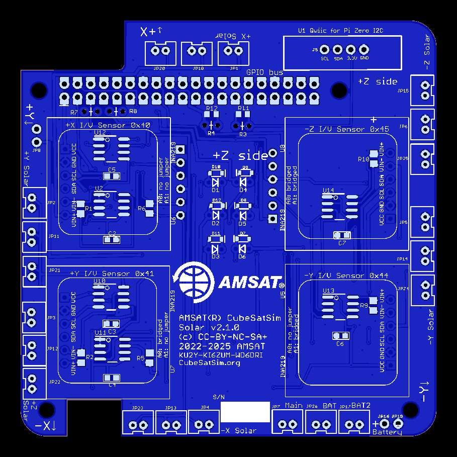
The solar board is a panel combiner with per-panel instrumentation:
- Per-panel current sensing: ~12× INA219 monitors (a mix of through-hole “purple board” INA219 modules and INA219AIDR chips), each reading one solar input through its own 0.1 Ω shunt (R100). This is what produces the satellite’s multi-channel current telemetry — you can watch each face’s contribution change as you shade the cube.
- Blocking diodes: Schottky
D1–D6 = 1N5817andD7–D12 = BAT20J(1 A / 23 V) OR the panels together and prevent reverse current into a shaded or cold panel — the same diode-OR a real satellite uses across its solar strings. - Panel connectors: a bank of Micro-JST 2-pin jacks (
JP1–JP26) for the panel leads — matching the kit’s 10 JST-terminated panels. - Bus:
4.7 kΩI²C pull-ups;JP9 = VDD-ENenable.
4. Inter-board interconnect
Two buses tie the stack together:
- The 20×2 GPIO stacking header (J1) — present on every board — carries power (
PI_3V3,BATT), the I²C telemetry bus (SDA/SCL), the FM/audio nets (AUDIO_IN/OUT,PTT,PD,FM,LPF,SQUELCH), serial (PI_TXD/RXD), and the LED/button lines (PI_LED1/2,PB). Boards literally stack and inherit these nets. - Micro-JST jumpers — carry battery and solar power/sense between the Battery, Solar, and Main boards (
BATT_IN/BATT_OUTand the panel feeds).
The result: the Pi/Pico read all V/I/temperature over one I²C bus, drive the FM module over serial + a PWM audio line, and the power flows panel → solar board → battery board → Main board → 5 V to the Pi, exactly the architecture Vol 1 sketched and Vol 2 explained.
References
Footnotes
-
CubeSatSim hardware v2.1 — schematics (
cubesatsim-{main,battery,solar}-v2.1.0_schematic.pdf) + BOMs — https://github.com/alanbjohnston/CubeSatSim/tree/master/hardware/v2.1. Local copies in02-inputs/research/schematics/. Board files © CC-BY-NC-SA AMSAT. ↩